With the increasing demand of computation-intensive applications and large-scale data processing, network devices such as servers need a stable supply of high-current to support high-performance computing. With the significant increase in power demand, power systems must have efficient overcurrent protection and monitoring capabilities.
Traditional high-current power protection schemes usually rely on multiple discrete devices. However, in high-power application scenarios, they face problems such as increased design complexity, excessive space occupation and maintenance difficulties. In order to meet the demand of smaller board area, the number of components used is continuously reduced. As time-to-market decreases, engineers need to find ways to simplify design. Changgong Micro provides an innovative solution to the above design challenges.
IVS introduces the 50A highly integrated E-Fuse -- IS6105A, a chip designed for hot-swap protection, which can effectively protect the input from output short circuits and transient effects. During startup, the surge current can be limited by setting the output voltage rise slope. IS6105A built-in MOSFET and sampling resistor, and equipped with PMBus digital communication interface, power protection, monitoring and control functions are highly integrated in a single silicon chip. The system design is simplified by minimizing the number of external components used while efficiently handling high current loads.
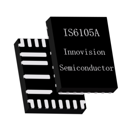
IS6105A supports 4V-16V wide voltage input, equipped with current monitoring function (IMON), and uses an integrated power MOSFET with RDS_ON of 1.2mΩ, built-in advanced on-chip current sampling technology, which can quickly and accurately detect current. The auxiliary discharge function of external output capacitor energy is set inside the chip. When the protection is triggered and the enable is closed, the output can be reduced faster and the back-end loop can be closed to realize the fast power down of the load circuit in the abnormal state and achieve the function of the protection circuit.
Highly integrated
IS6105A highly integrates the functions of various discrete devices into the size of 4mm x 5mm. The chip also integrates a comprehensive control function module, a high-precision detection module and a low-internal resistance high-rate conduction MOSFET. Compared with the discrete combination, the chip can reduce the number of peripheral parts, reduce the design space and cost.

Figure: IS6105A versus discrete hotplug solutions
Compatible with PMBus protocol communication
IS6105A is compatible with PMBus 1.3 standard, which can provide simple and flexible configuration, accurate system control of the circuit board and specific monitoring and telemetry technology. The PMBus interface allows programming a variety of parameters, such as voltage, current, temperature and fault parameters, and reads and reports real-time information. Users can dynamically adjust these parameters in order to quickly and easily integrate power information for more efficient power management, which meets the multiple needs of data centers for high current, high performance protection and system simplification. As shown in the following figure, IS6105A modifies the protection mode example of OVP through PMBus:
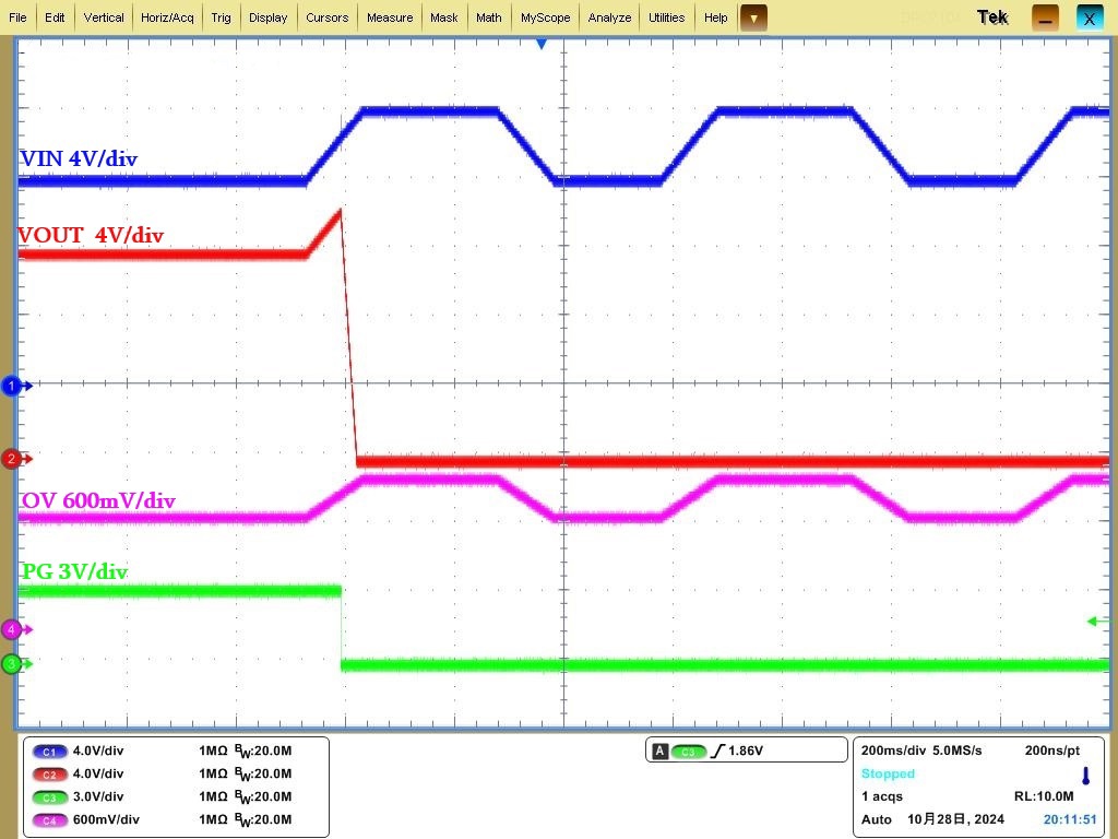
Figure: OVP is set to LATCH mode by PMBus

Figure: OVP is set to RETRY mode by PMBus
Comprehensive high precision current and voltage signal acquisition
While supporting PMBus protocol to read real-time voltage and current size, IS6105A can quickly obtain real-time voltage (VIN/VOUT), current (IOUT), Temperature (Temperature), power (PIN) and other data through the internal high-precision voltage and current acquisition module, and make response adjustment. In the circuit application without PMBus communication, the IS6105A can generate a voltage proportional to the device current through the external resistance of the IMON pin to ground, so as to realize the current value monitoring and feedback.
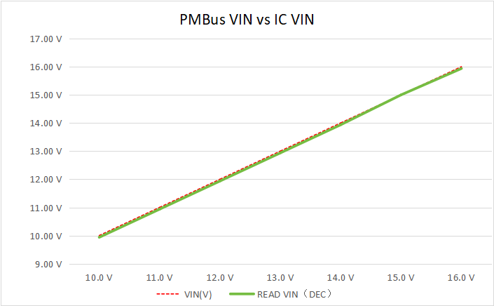
Figure: VIN accuracy is ±1% of the range range
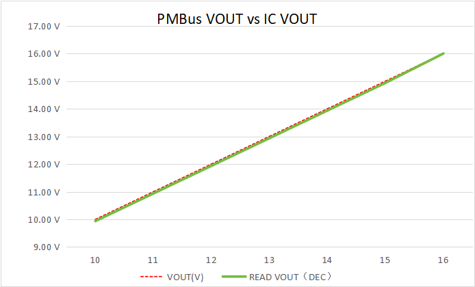
Figure: VOUT accuracy is ±1% of the range range
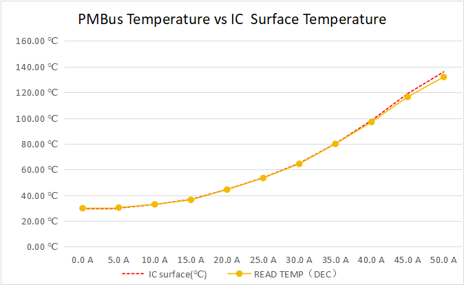
Figure: Temperature accuracy within the range of ±3%
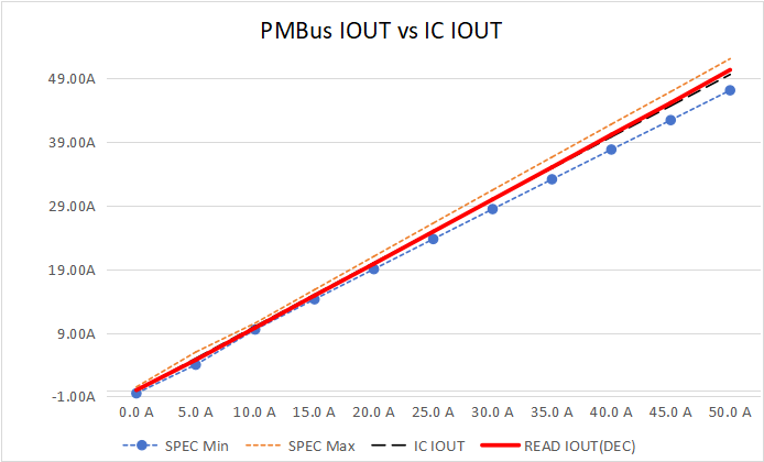
Figure: The PMBus IOUT accuracy is within ±5% of the range
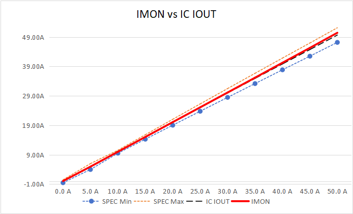
Figure: The Imon accuracy is 10A-50A ±3% of the range range
Support for Hot plug applications
As with many communication infrastructures, high availability and reliability are key elements of data center system design. Pluggable modules and PCBS (such as servers and storage devices) require protection and control circuitry at the power interface, often referred to as hotplug control circuitry.
In the application of Hot plug, the input terminal will generate extremely high voltage at the moment of hot plug, and there is a risk of overvoltage breakdown of the back-end device. In order to prevent the instantaneous high voltage conduction to the back-end of E-Fuse and cause device damage, it should be avoided to power on immediately after insertion and wait as much as possible for the input voltage to be stable before powering on. IS6105A supports users to delay chip startup by preset insertion delay to avoid jitter voltage at the moment of insertion. From the insertion instant, timer will enter the insertion delay count. When the timer count ends and the power-on condition is satisfied, VOUT will start soft start. The insertion delay is introduced by timer counting, which can effectively avoid the risk of overvoltage breakdown caused by unstable voltage at the moment of insertion.
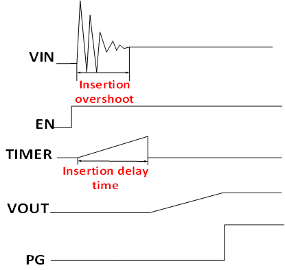
Figure: IS6105A hotplug boot diagram
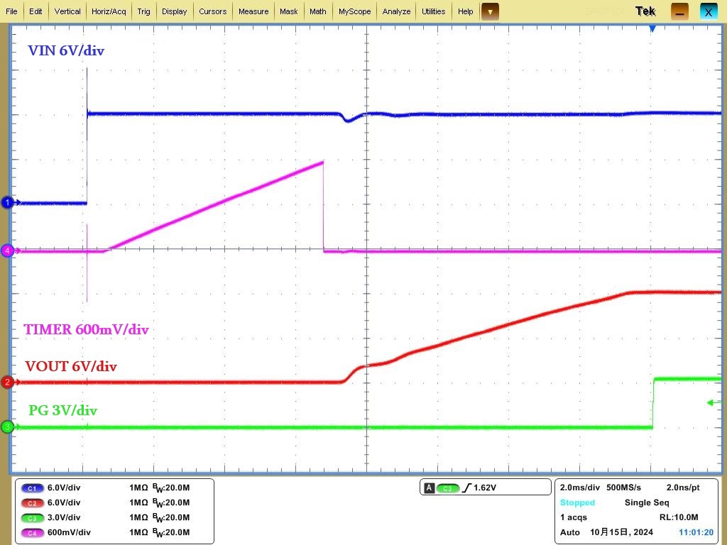
Figure: Schematic diagram of the hotplug startup waveform of the IS6105A
High-speed fault response
To avoid the shutdown caused by short circuit or overload of the load power supply and the device, the user can set the maximum current limit of the E-Fuse through the ISET pin. When the current is monitored to exceed the set value, the system will limit the current and perform fault timing. If the current drops to the normal value within the timing, the chip can exit the OC state in time to RECOVER. If the current fails to fall below the set value after the timing, the chip will turn off the current limit function, pull down through the fault reporting pin, and quickly cut off the loop (OCP).

Figure: Schematic diagram of IS6105A overcurrent protection and overcurrent recovery
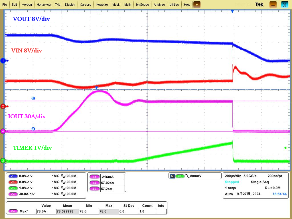
Figure: Schematic diagram of the OCP measured waveform of the IS6105A
For instantaneity large currents with faster uplift and larger current values, the IS6105A will immediately trigger the SCP protection, allowing the reaction to be made and the FET to be turned off within 200ns. After the set time interval, the self-recovery current limiting power on is attempted. If it fails to exit the overcurrent state, the chip will no longer be powered on and enter the latch mode to wait for the user to troubleshoot and manually restart.
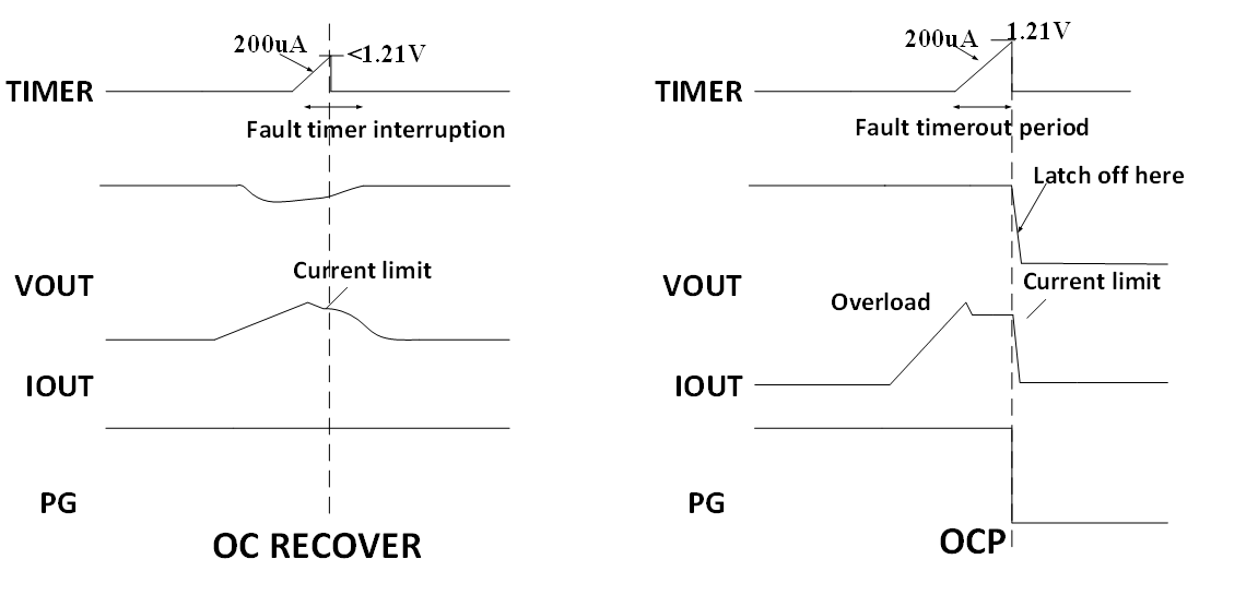
Figure: Schematic diagram of the short circuit current of IS6105A
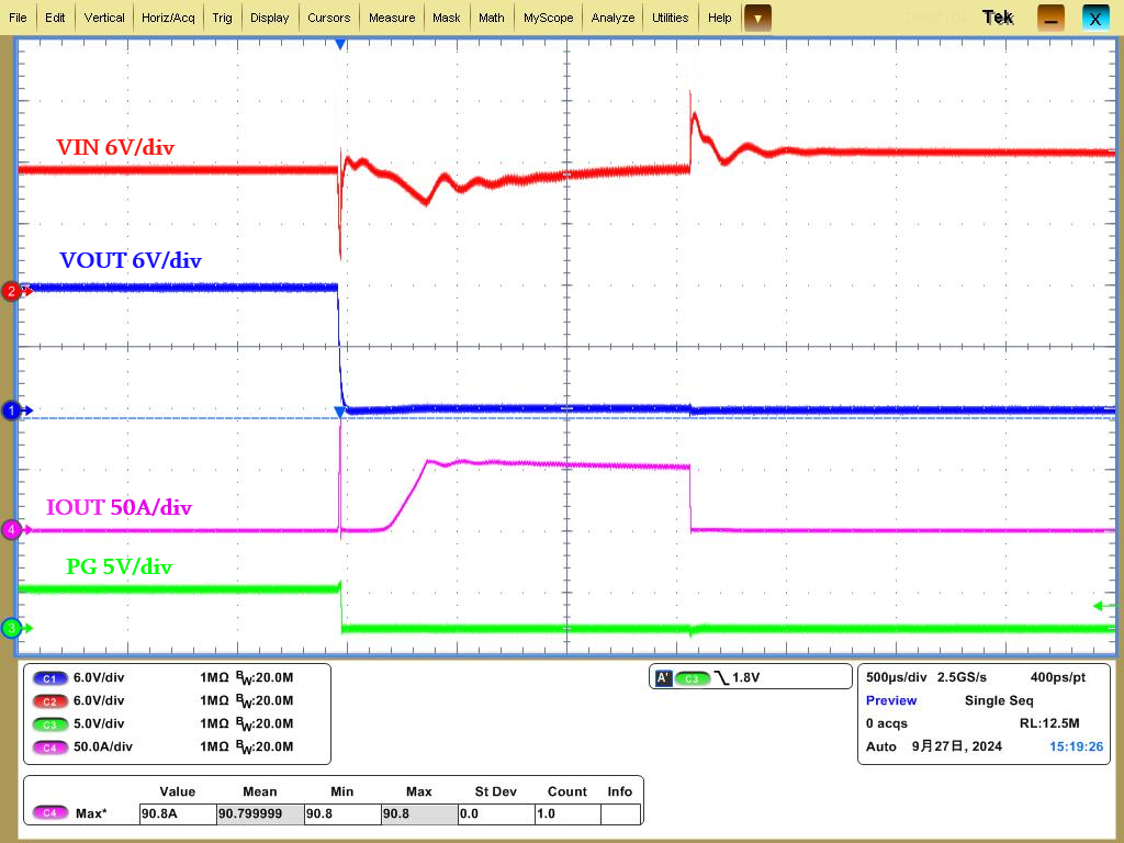
Figure: Schematic diagram of the measured SCP waveform of IS6105A
Ample Safe Workspace (SOA)
MOSFET is the key to the operation of E-Fuse, and the parameters of its safe operating region (SOA) determine the upper limit of the electrical performance of E-Fuse. Having a larger SOA means that the chip can operate safely and stably over a wider range of electricity and currents. The following figure shows the SOA of IS6105A. As an E-Fuse supporting constant pull load of 50A, the limit current of IS6105A is 110A, which leaves an extremely abundant current margin. When the instantaneous high current flows through, IS6105A can still work normally.
To prevent the oversized VDS stacking IDS beyond the SOA before MOSFET conduction. IS6105A has perfect prevention function. Inside the chip, in addition to using soft start to suppress surge, the current limit of soft start power on is also set to ensure that the MOS works within the SOA.
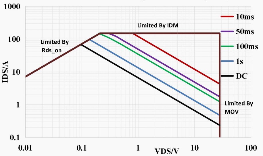
Figure: IS6105A Safe Work Area (SOA) diagram

