1. Product guide
IS6608A, The first multi-phase parallel power supply chip for CPU power supply in China, which is compatible with PMBusTMHigh-frequency synchronous voltage-reduction converter of the interface. Using a 4mm x 5mm FCQFN-25 package, it can achieve an output current of up to 30A per phase in a wide input range, and can support up to 8 chips in parallel to achieve a peak output current of 240A. In the field of high-current applications, IS6608A enables excellent current sharing and phase interleaving functions, minimizing the use of existing
芯片类别 | DC/DC降压变换器 |
规格型号 | IS6608A |
输入电压 | 3.3V-16V |
输出电压 | 0.4V-5.5V |
输出电流 | MAX 30A |
电压精度 | 0.5% |
频率 | 400kHz,600kHz,800kHz,1MHz |
并联相数 | MAX 8相 |
效率 | 90%以上 |
工作温度范围 | -40ºC至125ºC |
应用场景 | 服务器、台式机、笔电、基站等 |
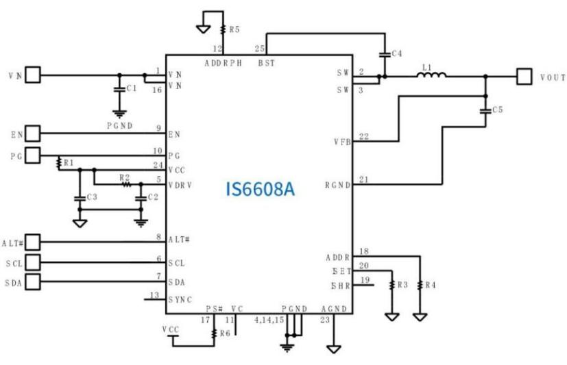
Figure IS6608A Typical circuit diagram
IS6608A The GUI and peripheral circuit configuration can be modified according to the diversification of terminal use scenarios, in order to help customers complete the product design and import, this article will systematically explain the use of the IS6608A instructions and layout suggestions, and simply and clearly introduce the matters needing attention in the use of the chip to the readers.
2. Use instructions for the GUI
IS6608A GUI It is a graphical user interface software tool independently developed by Changge Micro and used for supporting IS6608A design, which can help users to debug the internal configuration more quickly and intuitively. IS6608A GUI Following the PMBUS protocol, interact with IS6608A by USB-to-I²C (dongle).
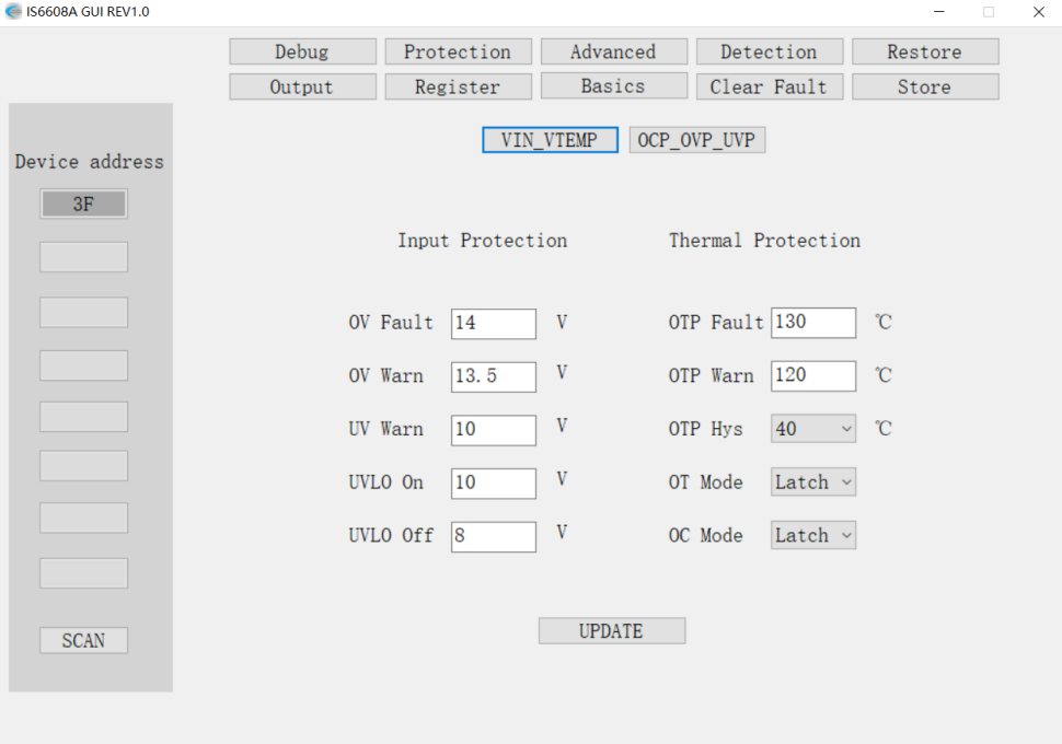
Figure IS6608A GUI Software use interface
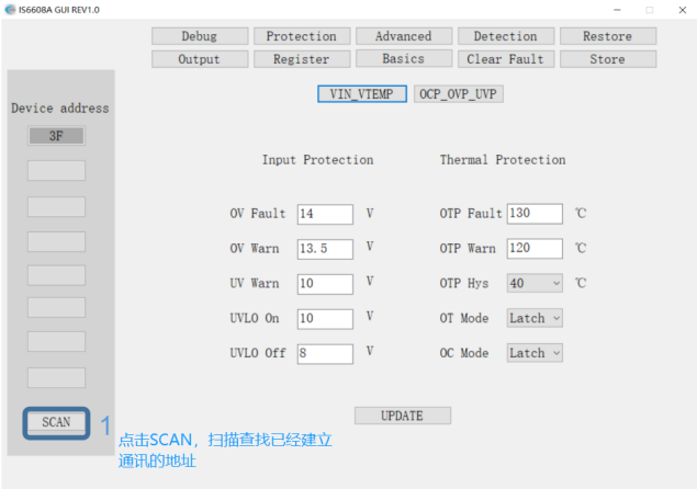
2.1.GUI write and burn steps
Step 1: Click SCAN to find the established mailing address
Step 2: Select the required mailing address
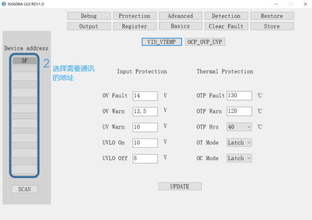
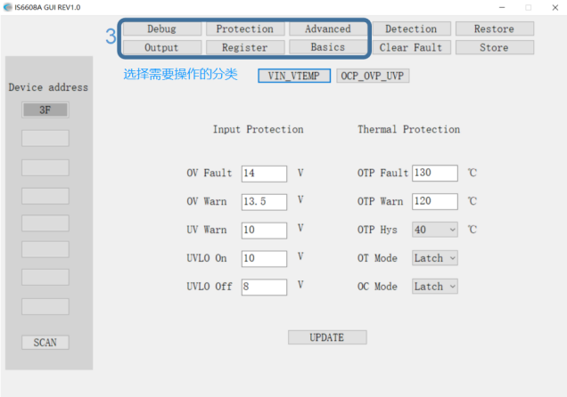
Step 3: Select the required operation classification
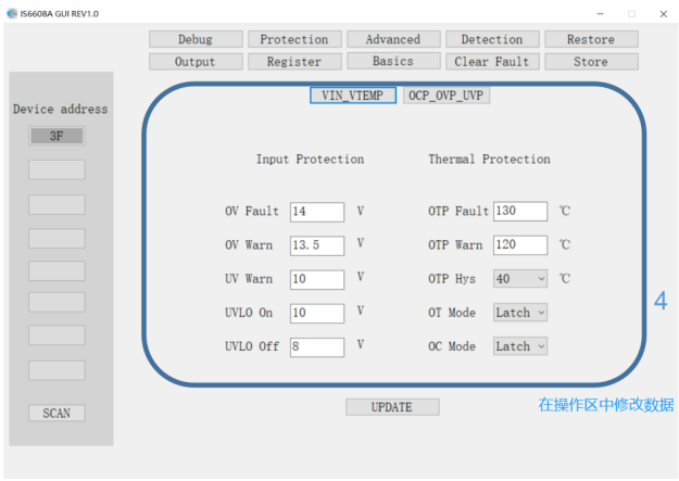
Step 4: Modify the data in the operation area
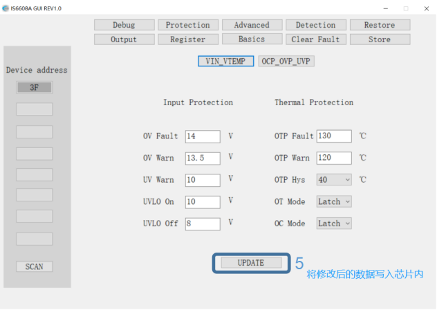
Step 5: Write the modified data into the chip
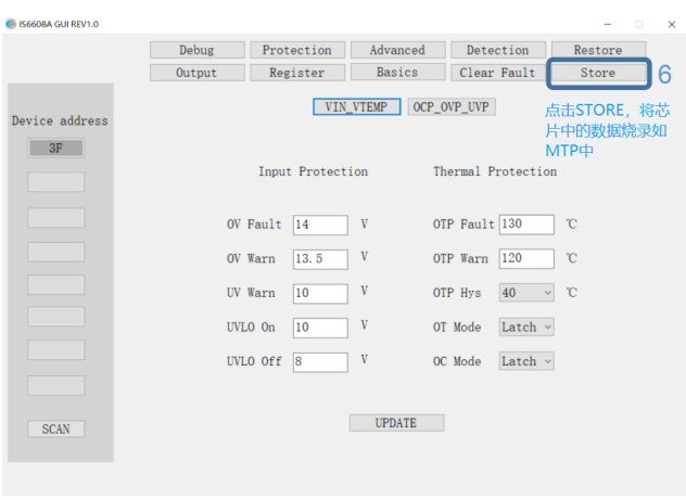
Step 6: Click STORE to input the chip data into the MTP
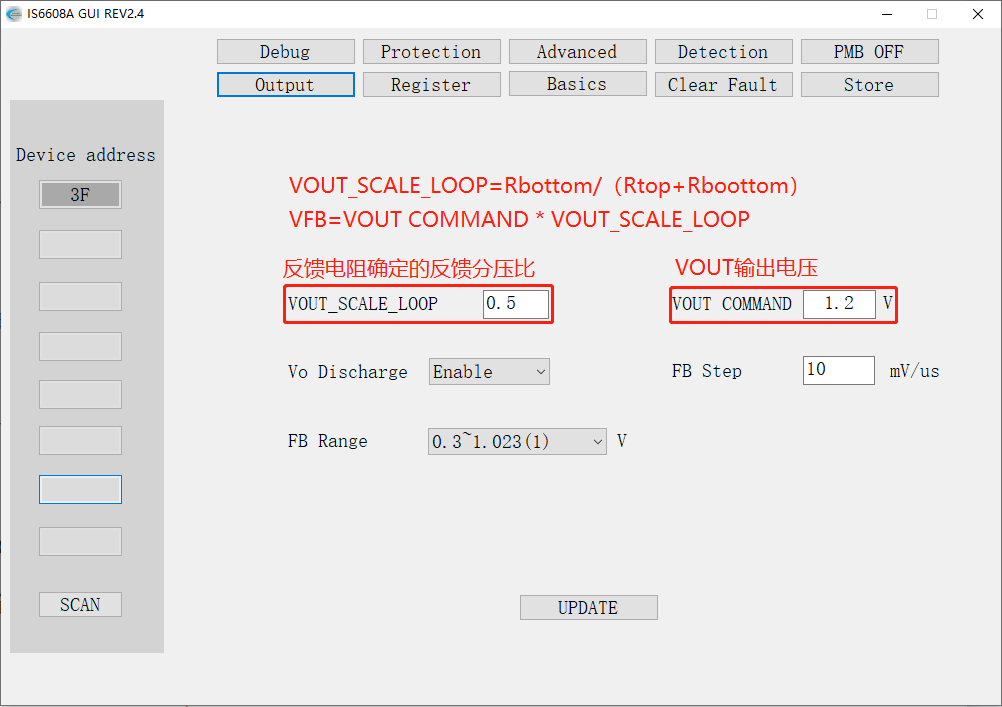
2.2 Output voltage adjustment
VOUT COMMAND And VOUT _ SCALE _ LOOP is used to set the VFB voltage with the formula:
For example Rtop=2kΩ,Rbottom=6kΩ,VOUT=0.8V, the output voltage step is as follows:
u According to Rtop = 2 kΩ, Rbottom = 6 kΩ, then VOUT _ SCALE _ LOOP = 6 kΩ / (2 kΩ + 6 kΩ) =0.75;
u VOUT=0.8V,VOUT COMMAND=0.8V;
u Click UPDATE to write the data to the register;
u Click the Store to deposit the data in the register into MTP, then VFB=0.8V*0.75=0.6V.
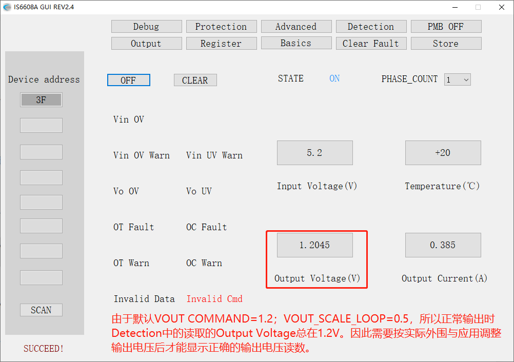
2.3 Read out of the VOUT values
The actual read value of chip VOUT voltage read is VFB voltage. If the correct output voltage is required in Detection, VOUT COMMAND should be configured with VOUT _ SCALE _ LOOP to display the correct value.
Example the application of the Rtop=2kΩ,Rbottom=6kΩ,VOUT=0.8V by reading the output voltage step as follows:
u According to Rtop = 2 kΩ, Rbottom = 6 kΩ, then VOUT _ SCALE _ LOOP = 6 kΩ / (2 kΩ + 6 kΩ) =0.75;
u VOUT=0.8V,VOUT COMMAND=0.8V;
u Click UPDATE to write the data to the register;
u Click Detection to read the correct VOUT voltage on the GUI.
Note: The accuracy of the external VFB partial voltage resistance can affect the accuracy of the VOUT reads.
IS6608A With perfect protection functions, including overcurrent protection (OCP), negative overcurrent protection (NOCP), over pressure protection (OVP), undervoltage locking (UVLO) and over temperature protection (OTP) and other protection mechanisms, used in the failure or accident action and abnormal, the protection chip is not damaged.
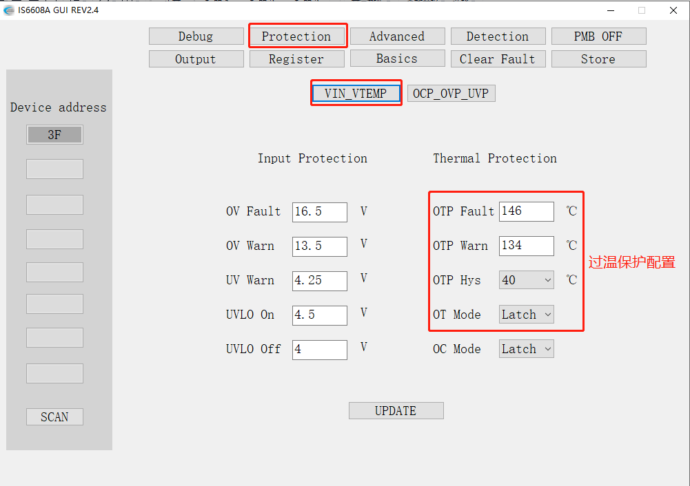
2.4 OTP protection mode setting
The default OTP protection temperature for the latest version of IC is 146℃. The protection mode can be selected in Latch and Retry [hysteresis temperature including RETRY], and the default is Latch. The following figure shows the modification steps:
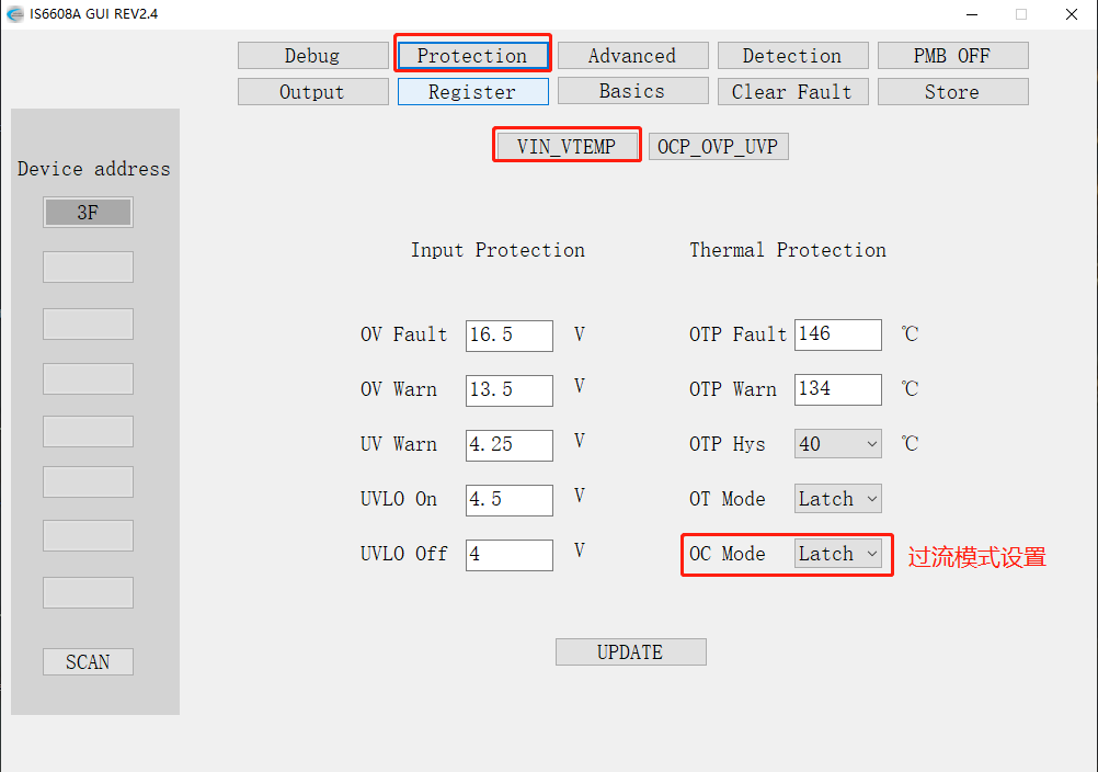
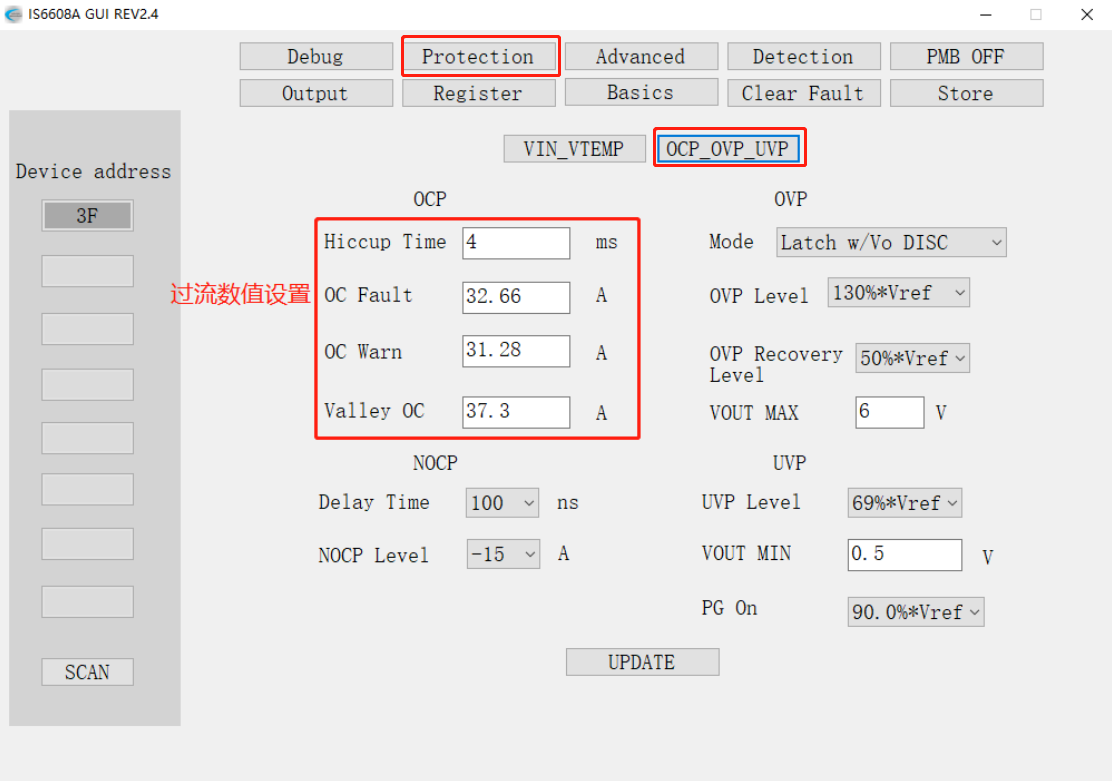
2.5 Setting of the OCP protection mode
The default DC protection current is 32.66A, and the protection mode can be selected in Latch and Retry [Hiccup Time including Retry], and the default is Latch. The following figure shows the modification steps:
2.6 Setting of the OVP protection mode
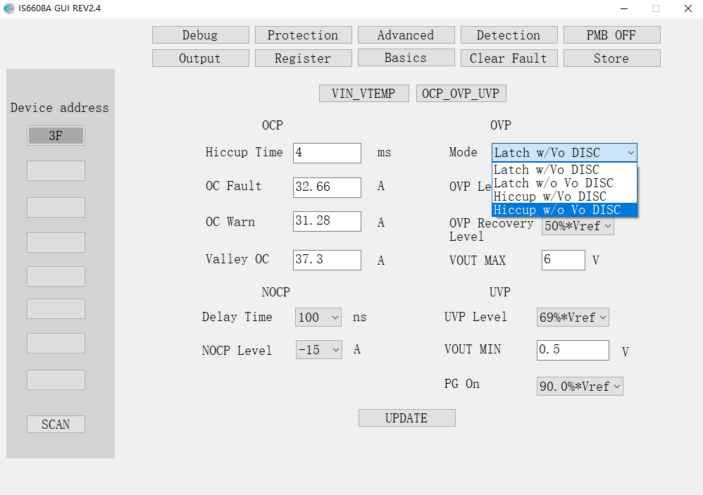
The default overvoltage protection value is 130% * Vref, the protection mode can be selected in Latch and Retry [including recovery voltage and protection mode of Retry], the default is Latch. The following figure shows the modification steps:
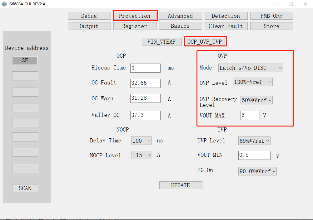
There are four response configurations for OVP protection mode, namely Latch & Hiccup and w / Vo DISC & w / o Vo DISC, as follows:
u Latch: After overvoltage, the power lock, needs to restart manually
u Hiccup: When the overvoltage protection is triggered, it will drop to the
u voltage set by OVPRecovery Level and power on again;
u W / Vo DISC: When the overvoltage protection is triggered, the VoDischarg function is used to pull down the output voltage;
u W / o Vo DISC: When the overvoltage protection is triggered, reduce the output voltage without using the Vo Discharg function.
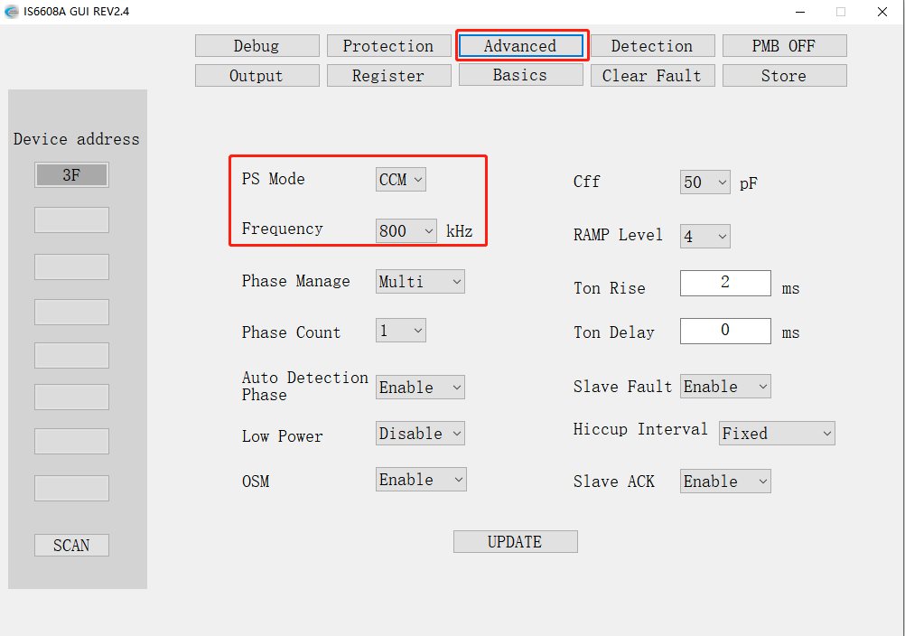
2.7 芯片工作频率和模式的设置
The default operating frequency of the chip is 800 kHz, and the default operating mode is FCCM. The following figure shows the classification of function settings:
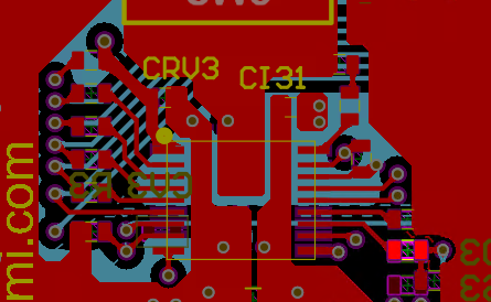
3. Route / layout suggestions
IS6608A The periphery contains a variety of functional pin configurations, which have high requirements for IC routing and element placement. Good peripheral routing / layout can effectively affect the working efficiency and stability of the chip. In addition, the peripheral circuits can also provide good electromagnetic compatibility, noise reduction and anti-interference ability.
It is worth noting that in the absence of specific requirements, GUI is not essential for the use of IS6608A, but routing / layout is one of the things that users need to pay attention to. Route / layout recommendations are as follows:
1. 3K resistance per phase ISHR pin in the near end of multiphase parallel;
2. Place a sufficient amount of VIA directly below the chip and the VIN / GND pin as possible;
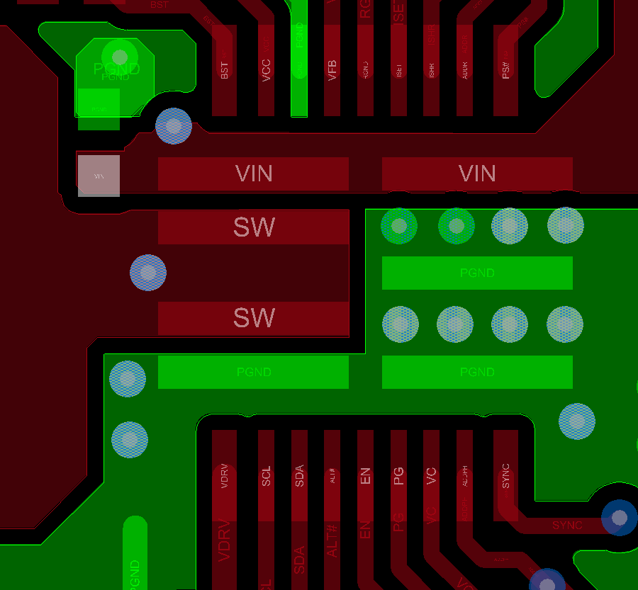
3. 1uF 0402 small capacitor filter;
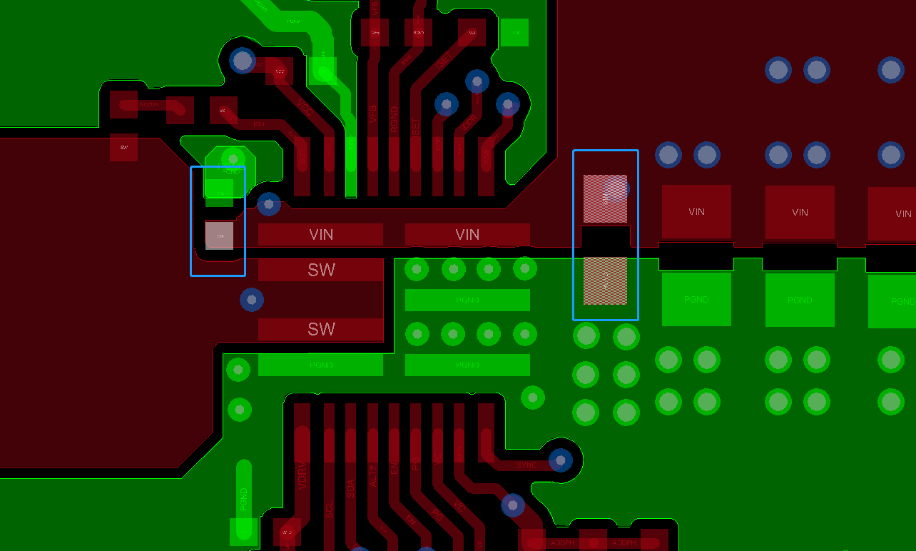
4. Sensitive routing [such as VFB-RGND / SYNC / ISHR / VC] need to avoid interference signals [such as SW / BST / VIN] placed;
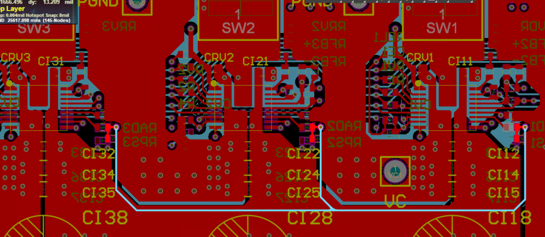
5. The BST circuit is as short as possible;
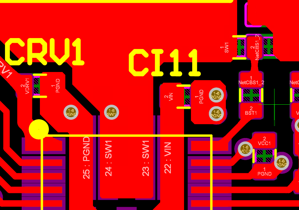
6. VC C/V DRV capacitor should be placed as close to the pin as far as possible;
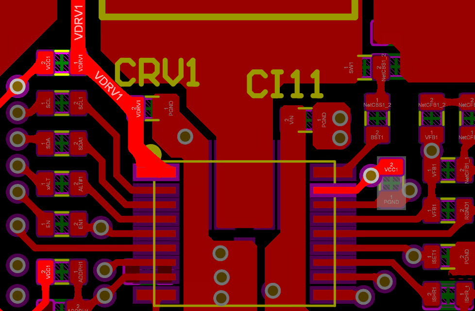
7. The ISET / ADDR / ADDPH resistance is placed as close to the pin as possible and requires a 1% precision resistance;
[About US]
Innovision Semiconductor Inc. was founded in May 2016, located in Songshan Lake, Dongguan, has a professional technical team, adhere to independent forward research and development, committed to high performance low voltage high current power chip design. In view of the domestic gap in the field of CPU power supply, a full set of solutions, breaking the status quo of foreign chip monopoly. Products include switching power supply, multi-phase controller, intelligent power level, power module, etc., which can be widely used in server, computer, communications, consumer electronics and other markets.
