一、 Product guide
IS6201A is a dual output digital multi-phase step-down controller, designed for CPU voltage regulation, and fully in line with PMBus 1.3.1 specifications, using 7mm 7mm QFN-56 package, can be matched with up to 8 long work micro self-developed 30A / 70A / 90 / 90A three current specifications of DrMOS, can be stable output of large current.
IS6201A Use the long industrial micro unique patent turbine constant conduction time (TCOTTM) Control algorithms to achieve a lightning-like fast transient response. It includes proprietary efficiency shaping techniques that can achieve superior efficiency across the entire load range. The dynamic phase control function can increase / decrease the phase according to the load current.

Figure 1 The information for the basic specification of the IS6201A
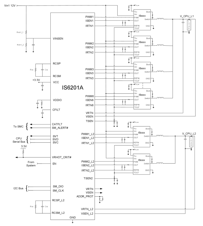
Figure 2 IS6201A Typical line diagram
IS6201A is also compatible with PMBus and AMD SVI2 digital communication protocol. Users can set the output voltage of the chip, read the output voltage and other functions of the chip through PMBus and AMD SVI2 communication. In order to help customers complete the product design import more quickly and conveniently, this article will systematically explain the use instructions and layout suggestions of IS6201A, and simply introduce the matters needing attention of the chip in the use process to the readers.
二、 GUI direction for use
IS6201A Support the SMBus / PMBus system interface, which can be easily configured with the GUI. GUI is a graphical user interface software tool independently developed by Changyu Micro and used for supporting IS6201A design, which can help users to debug the internal configuration more quickly and intuitively. IS6201A GUI Follow the PMBus protocol and interact with the IS6201A chip by USB-to-I2C (Dongle).
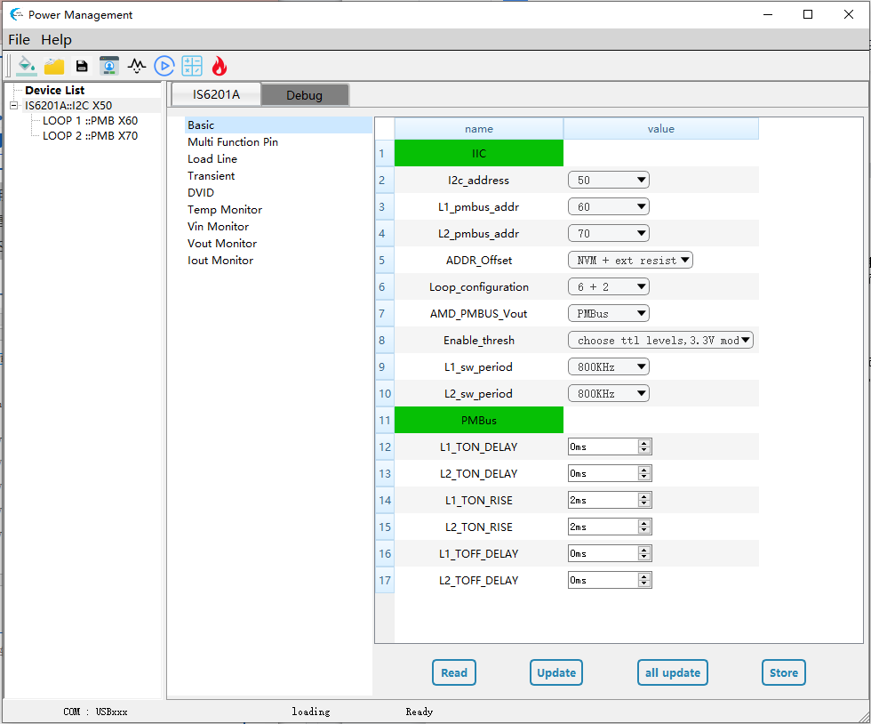
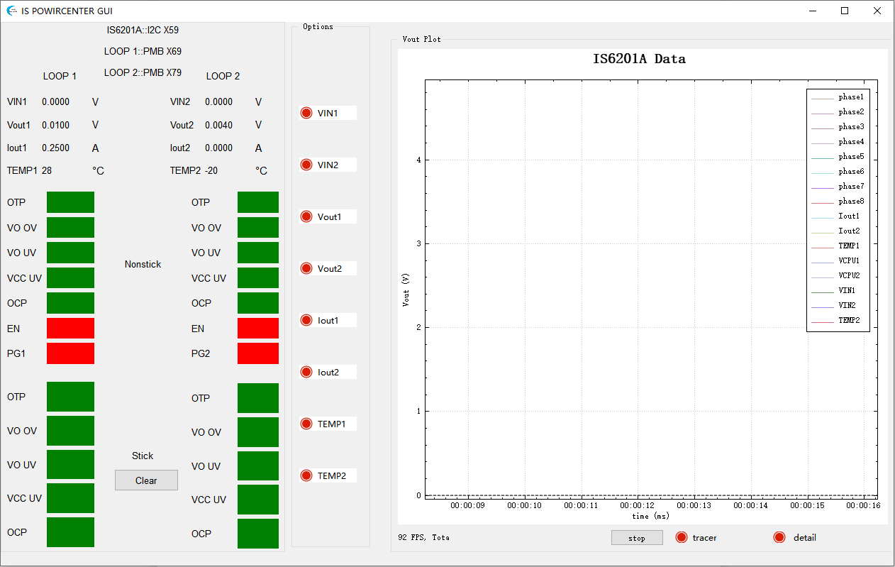
Figure 3 IS6201A GUI for the software usage interface
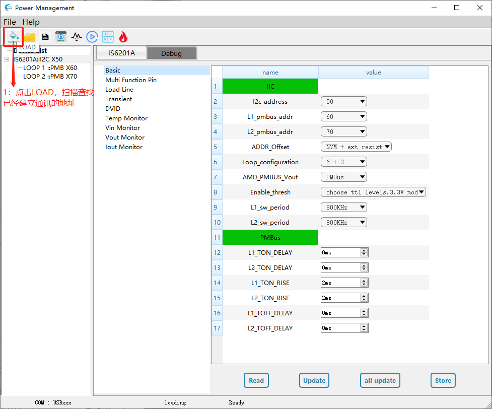
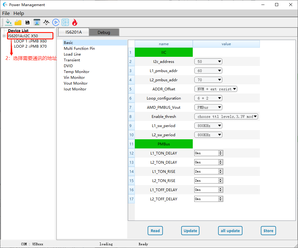
1. The GUI write and burn steps
Step 1: Click LOAD to scan the address for the recommended communication;
Step 2: Select the address that you need to communicate with;
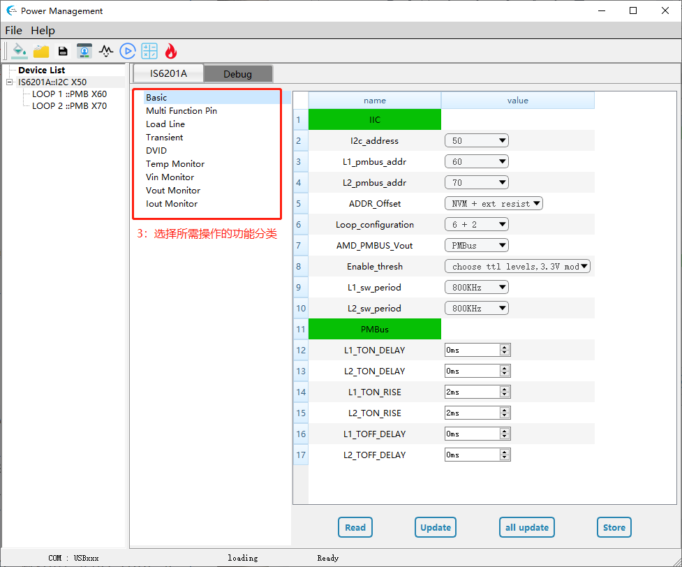
Step 3: Select the functional classification of the required operations;
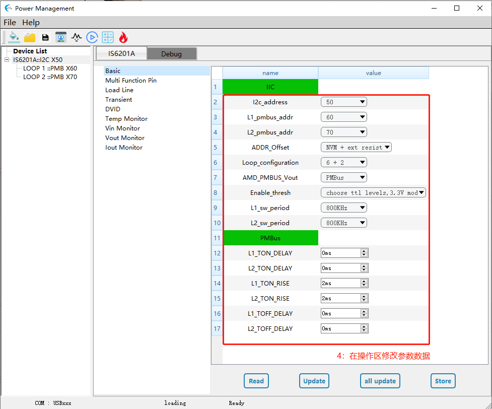
Step 4: Modify the parameter data in the operation area;
Step 5: Write the modified data into the chip;

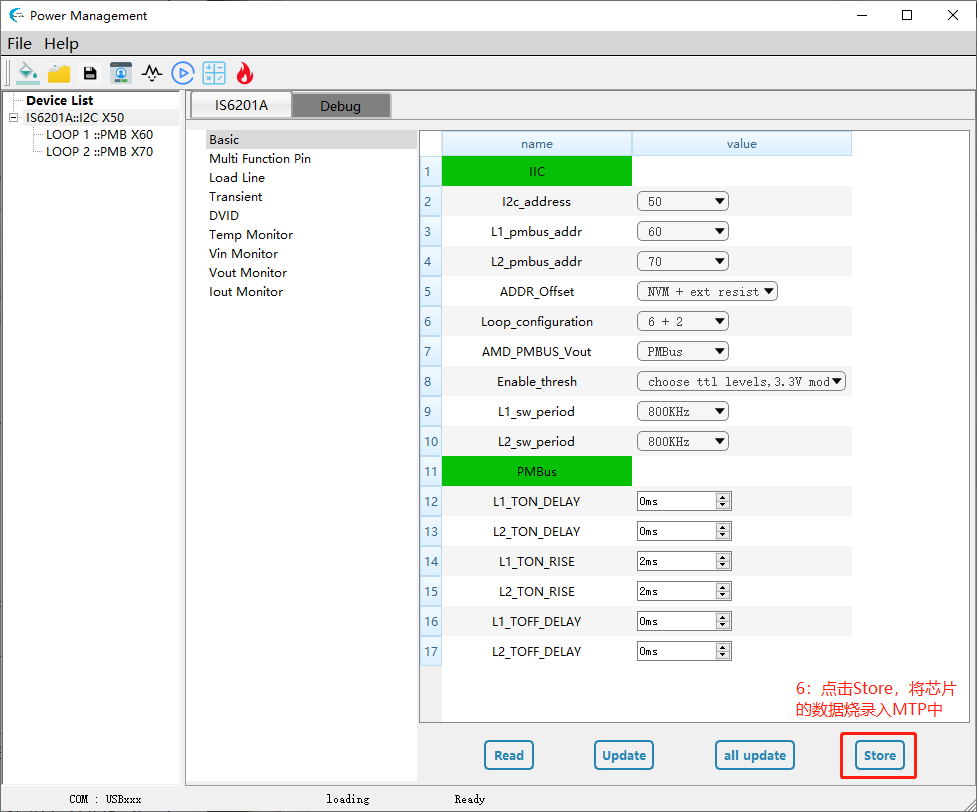
Step 6: Click Store to burn the data in the chip into MTP.
2. Output voltage adjustment
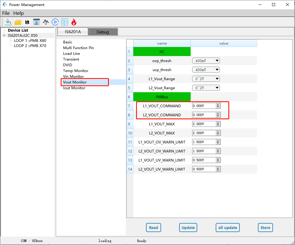
In PMBus mode, if you need to modify the output voltage value of two Loop, modify the required output voltage value into the corresponding VOUT _ COMMAND, and then click the Update button to complete the writing.
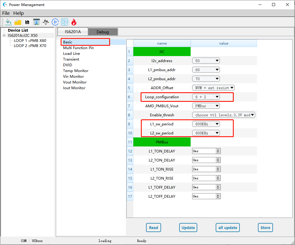
3. Output phase number and frequency adjustment
Change the phase number application combination of two Loops, modify the Loop _ configuration; If you need to change the switching frequency of both Loops, modify the L 1 _ sw _ period / L 2 _ sw _ period, and click the Update button to complete the writing. The default switching frequency is all at 800 kHz.
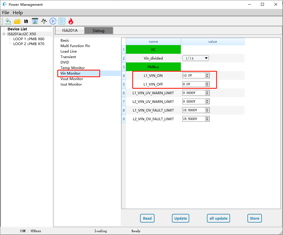
4. Input the threshold voltage adjustment
The default input voltage start threshold is 10V and close threshold is 8V; modify L 1 _ VIN _ ON (start threshold), L 1 _ VIN _ OFF (close threshold); note the lag between the two thresholds.
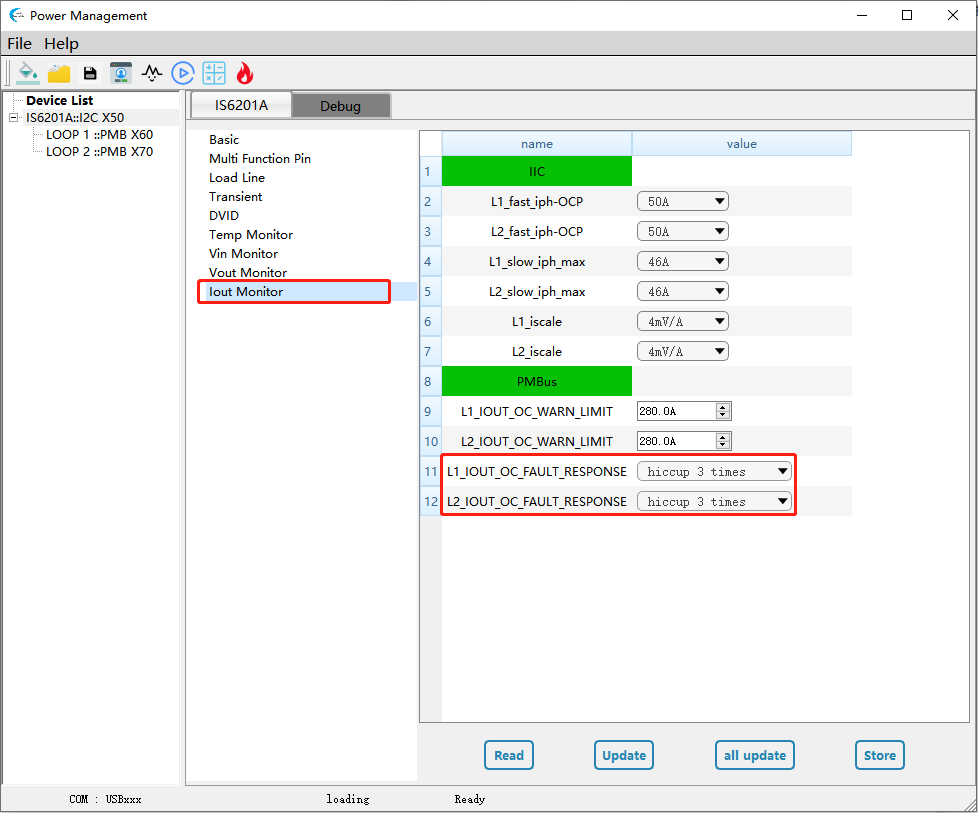
5.The OCP protection mode setting
The protection mode can be selected in shutdown and hiccup (including hiccup time); the default OC protection mode is hiccup 3 times.
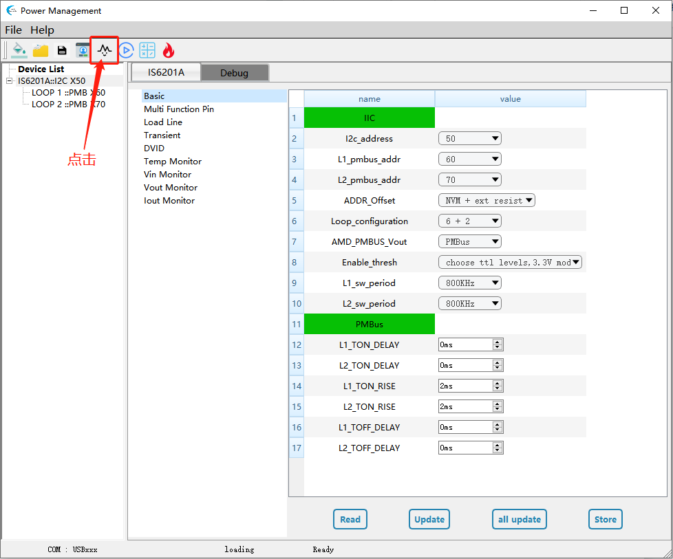
6. Read back the signal status monitoring
After clicking the LOAD scan to find the address of the recommended communication device, then open the read-back signal monitoring interface for real-time monitoring of signal data.
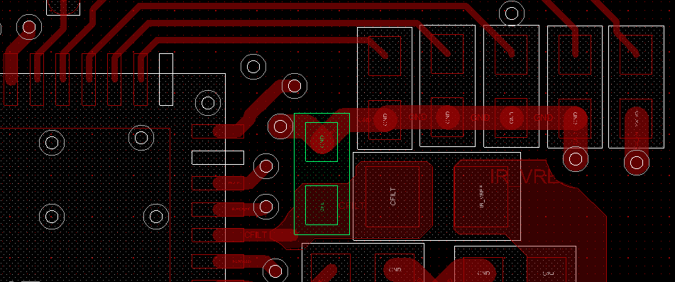
三、Wting / layout recommendations
Good peripheral routing / layout can effectively affect the work efficiency and signal feedback of the chip. It is worth noting that GUI is not a necessity for IS6201A use in the absence of specific requirements, but routing / layout is one of the things that users need to pay attention to. Taking IS6201A with DrMOS IS6806A as an example, the routing / layout suggestions are as follows:
1.IS6201A shall not be placed on the high current path; the 12V copper foil is not supported under the IC to avoid interference to the IC.
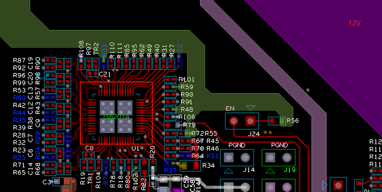
2. The capacitors of both VCC (Pin 38) and VCCM (Pin 41) need to be placed at the same layer near the end of the power supply pin; the line width of both VCC and VCCM remains 20 mil.
3. Current detection signal ISENx, IRTNx is sensitive routing, and the routing requirements are relatively strict:
① You need to return the difference line from the DrMOS end to the IS6201A;
② Keep the spacing with the nearby line or Via with large interference (> 25 mil);
③ When changing the signal line, try not to pass through the copper foil with large interference such as 12V, otherwise maintain a large gap;
④ The filter capacitance between ISEN and IRTN is placed in the same layer as the IC, close to the Pin foot.
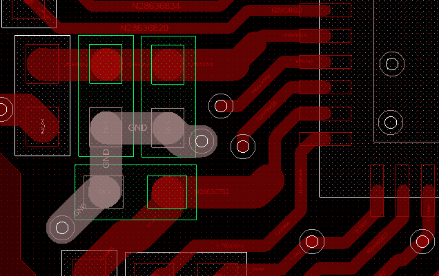
4. Voltage feedback signal VSEN, VRTN is a sensitive line, with the following suggestions:
① Walk a pair of difference lines from the load end back to IS6201A;
② Need to keep spacing from nearby large lines or Via (> 25 mil);
③ When changing the signal line, it is recommended not to pass through the copper foil with large interference such as 12V, otherwise maintain a large gap;
④ The filter capacitor is placed in the same layer as the IC, close to the Pin foot.
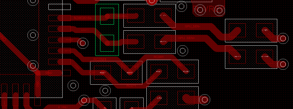
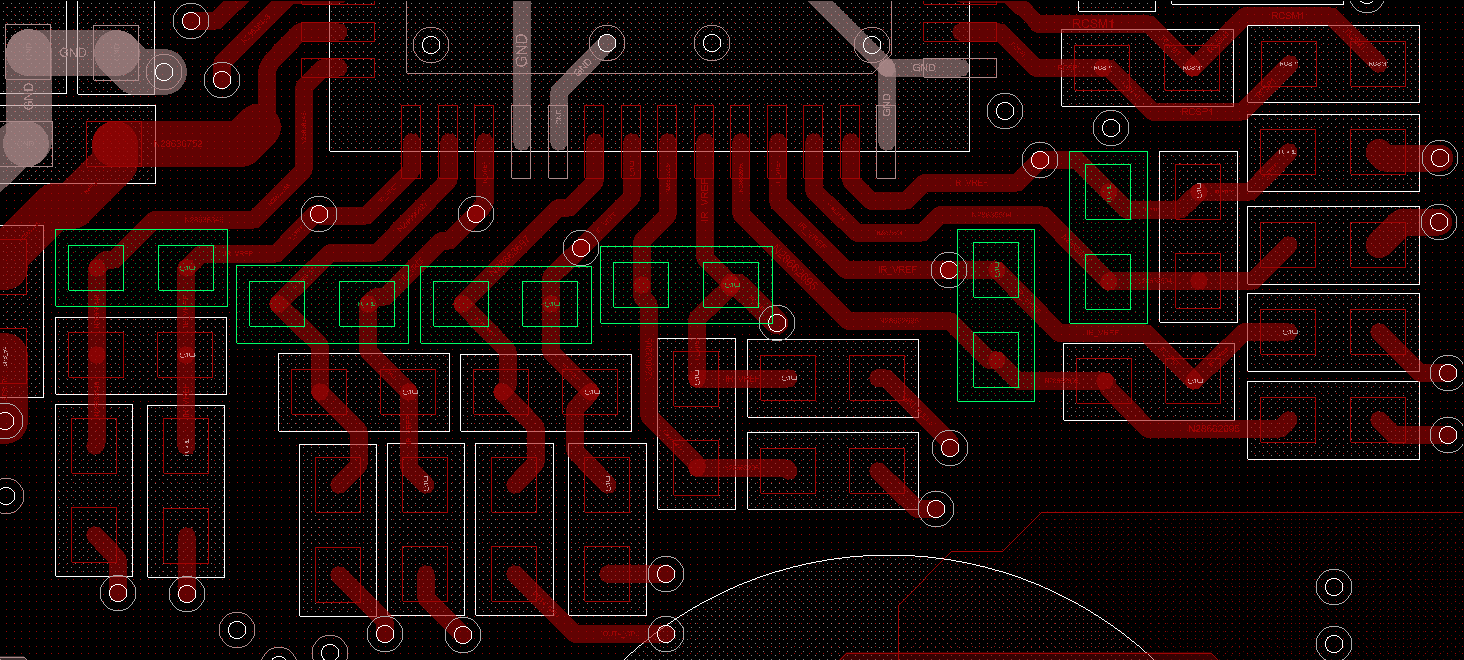
5. Temperature detection signal TSENx is sensitive routing, with the following suggestions:
① TMON signals of all phases (the same Loop) together and back to IS6201A,
② Keep spacing from nearby interfering wires or Via (> 25 mil).
6. PWM signal is a signal with strong interference ability, with the following suggestions:
① Need to pay attention to avoid sensitive wiring, maintain a large spacing;
② Keep the spacing between the PWM signals;
③ The line width is recommended for 8-10 mil.
7. The capacitance of CFILT (Pin 10) is placed at the proximal end of the pin.
[About IVS]
IVS was founded in May 2016, located in Songshan Lake, Dongguan, has a professional technical team, adhere to independent forward research and development, committed to high performance low voltage high current power chip design. In view of the domestic gap in the field of CPU power supply, a full set of solutions, breaking the status quo of foreign chip monopoly. Products include switching power supply, multi-phase controller, intelligent power level, power module, etc., which can be widely used in server, computer, communications, consumer electronics and other markets.
