With the rapid development of big data and Internet of things, the demand for communication base stations and data centers is growing geometrically. In order to adapt to the rapid development of communication equipment and data centers, DC-DC power management chips need to provide stable power output while providing high power density, high conversion efficiency and lower energy consumption. Therefore, the DC/DC power chip with high power density, high efficiency and high stability has become a key factor to ensure the performance and reliability of the communication base station.
IS6620A, a highly integrated non-isolated dual-output DC-DC converter, is introduced by Changindustry Micro. Through optimized circuit design, improved wafer production process and the use of the most advanced packaging technology, the power density and conversion efficiency of the device are higher, anti-interference ability is stronger, and output voltage is more stable. The device supports a wide input voltage range (4.5V-18V) and can be configured as two independent dual 6A or single dual phase 12A supplies. The product features are as follows:
Pseudo-Current Control Mode with internal compensation
Output current up to 6A dual output
Dual-phase single output with output current up to 12A
Output voltage range: 0.5V to 5.5V, 90% Max duty cycle
Synchronize to an external clock using SYNC
Selectable switching frequencies are 500KHz, 1MHz, 1.5MHz and 2MHz
Two mode selection pins (MODE1 and MODE2) are used to select switching frequency, configuration, clock phase delay, and internal compensation
Supports safe pre-biased startup
Internal integration of OCP, NOCP, OVP, UVP, OTP, soft start protection and other protection functions
3 mm x 5 mm, 25Pin FC-QFN package
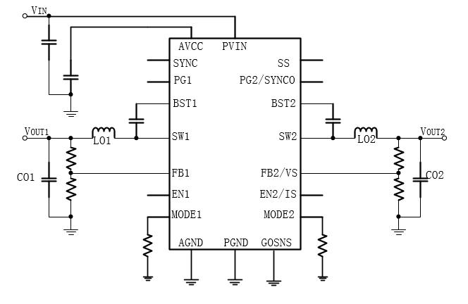
图1:IS6620A双路输出典型应用电路图
Technical Features
1. The control loop is simple and has strong anti-interference ability
Figure 2 shows the simple schematic diagram of the Pseudo-Current Control Mode (PCC) control mode, and Figure 3 shows the PCC control timing diagram. The input Vramp of the PWM comparator is generated through the Pseudo Current module and does not directly come from the sampling of the inductor current. It has a similar waveform as the inductor current IL, as shown in Figure 3. On the arrival of CLK signal, PWM signal becomes high, turn on the upper tube of power tube, Vramp rises linearly like inductor current, when it reaches VC, PWM flips to produce SHOT signal, PWM becomes low, turn off the upper tube of power tube, turn on the lower tube, until the next CLK comes again. PCC achieves fast dynamic response through nonlinear ramp compensation techniques of Vslp+ and Vslp-. In addition, the unique VC clamp technology enables smooth voltage conversion between DCM and CCM.
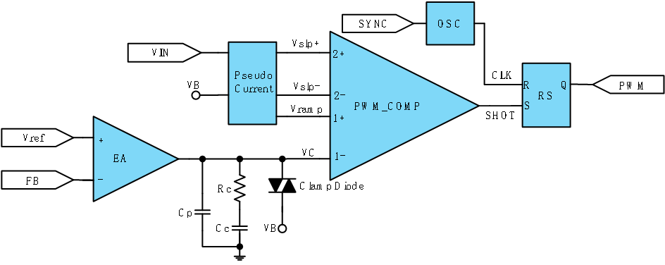
Figure 2: Schematic diagram of Pseudo Current Control (PCC) control mode
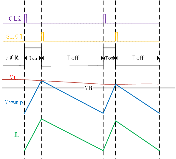
Figure 3: Timing diagram of Pseudo Current Control (PCC)
Compared with the traditional peak current control mode, the PCC control mode has better anti-interference ability, shorter Minimal on time, and can also achieve minimal jitter. Especially in the case of large current, the advantage of anti-interference ability is more obvious. Compared with COT control mode, PCC control mode uses a fixed frequency (CLK from the internal OSC or external SYNC signal), which is conducive to the synchronization of dual-phase parallel and phase stability control.
2. External CLK synchronization function, again improve the anti-interference ability of the system
When multiple switching power supplies are used at different frequencies, they will interfere with each other in the electromagnetic field, and also affect the normal work of other electronic equipment. After the frequency synchronization of the switching power supply, the output voltage and current waveforms of multiple switching power supplies are the same, which reduces the mutual interference between them and improves the anti-interference ability of the system. After the SYNC pin of the IS6620A chip receives the CLK signal of the system, in MR1 Mode, when the external input CLK signal with 50% duty cycle is within ±20% of the frequency set by the Mode pin, the working frequency of the IS6620A will be synchronized with the external CLK. If the SYNC signal is kept high, low or Float, the operating frequency of the IS6620A is generated by the internal OSC CLK to allow SW1 and SW2 to work with a 180° phase shift.
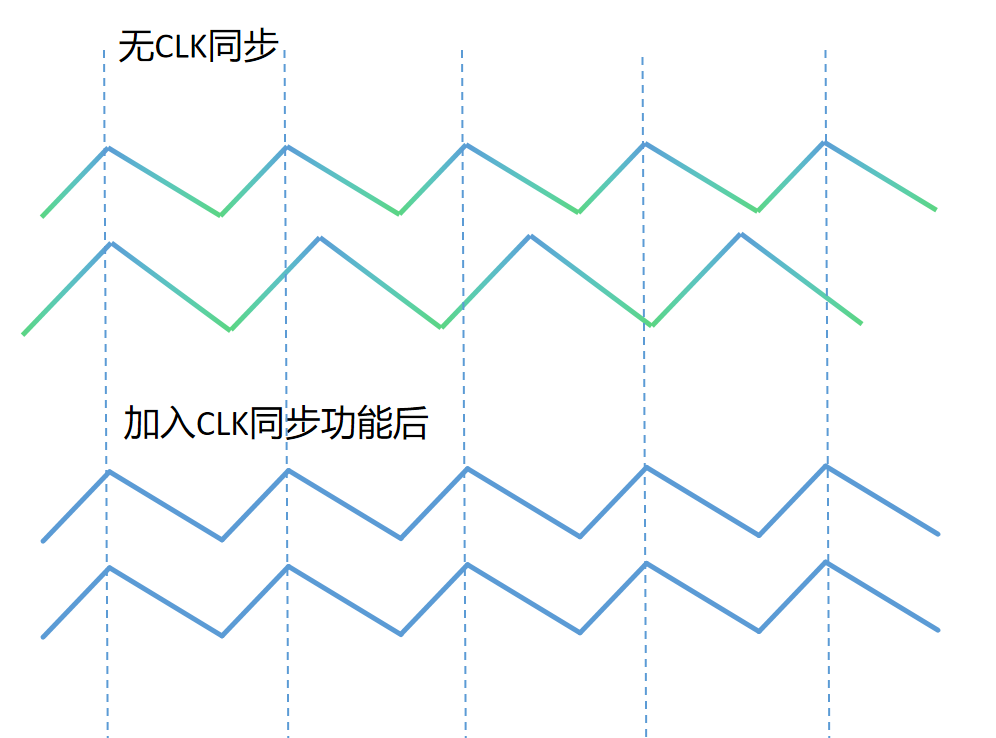
图4:有无CLK同步功能的2个Vout波形对比
Here is a configuration of a dual-phase single-output power supply for a synchronous external CLK:
The two Vouts of the chip are connected together.
The switching frequency is set by the external CLK received by the SYNC pin of the chip.
The phase shift of 2Phase is set by the chip Mode pin.
The GOSNS pin serves as the input to Remote sense.
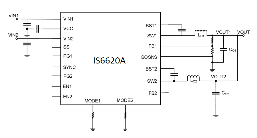
Figure 5: Schematic diagram of a dual-phase single-output power supply for a synchronized external CLK
3. Built-in integrator, high precision output voltage
IS6620A chip internal integrator function, can continue to modify the reference voltage Vref, so as to improve the output voltage in different loads, different input voltage and other conditions of voltage accuracy, output voltage accuracy up to ±1%.
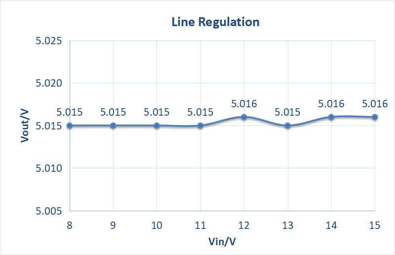
Figure 6: Linear adjustment curve diagram of IS6620A
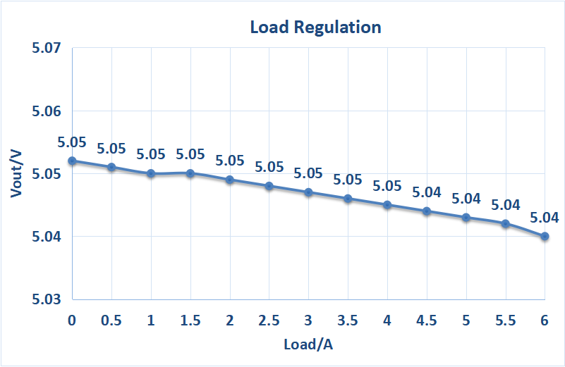
Figure 7: load adjustment curve diagram of IS6620A
4. High efficiency, low power consumption
Integrated with low on-resistance Rdson MOSFET (20mohm/8mohm HS/LS) and optimized drive current technology, the peak efficiency of IS6620A can reach 95.6% when Vin=12V and Vout=5V. Under the condition of light load, when the chip works in DCM mode, the loss of the chip can be further reduced and the overall efficiency of the chip can be improved.
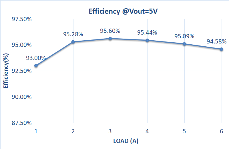
Figure 8: Efficiency curves of IS6620A at VIN=12V and VOUT=5V
Example Application Scenario
The input voltage of communication equipment is usually -48V, which is first converted to 12V by isolated DC/DC converter, and then converted to the voltage required by the main chip on the motherboard by non-isolated DC/DC converter. The following is an application design example of IS6620A power supply:
Application conditions: VIN=12V, VOUT1=1.2V(Imax=6A), VOUT2=1.0V(Imax=6A), Load Step: 0A~3A & 3A~6A, Vpeak-peak of VOUT1≤120mV(±5%), Vpeak-peak of VOUT2≤100mV(±5%).
Firstly, the switching frequency is selected. The switching frequency of IS6620A is 500KHz, 1MHz, 1.5MHz and 2MHz, and 1MHz is generally recommended.
Secondly, the inductance is determined, and the value is determined according to the current ripple of the inductor which is 20%~40% of the full-load output current. The full-load current of this application is 6A, so the current ripple of the inductor ranges from 1.2A to 2.4A. According to the formula ∆IL={(Vin-Vout) /L}*TON, combined with VOUT=1.2V, Fsw=1MHz, it is calculated that when VIN=12V, the inductance range is 0.45uH~0.9uH, VOUT=1.0V, Fsw=1MHz, VIN=12V, The inductance value ranges from 0.38uH to 0.76uH, and the final inductance value is 0.47uH.
Finally, according to the design tool provided by ChanggongMicro, the appropriate output capacitor is chosen for 1.2Vout and 1.0Vout respectively. Six ceramic capacitors of 22uF were selected for Vout=1.2V and six ceramic capacitors of 22uF were selected for Vout=1.0V. At this point, the key parameters of this application have been determined, and the following is the corresponding measured waveform.
Transient: VIN=12V, VOUT1 =1.2V, LOAD Step=3A, Slew rate=1A/us, Vpeak-peak=66.4mV.

Transient: VIN=12V , VOUT2=1.0V, LOAD Step=3A , Slew rate=1A/us, Vpeak-peak=64.8mV

Ripple: VIN=12V, VOUT1 =1.2V, LOAD=0A,6A Vripple=10.24mV

Ripple: VIN=12V, VOUT2 =1.0V, LOAD=0A,6A Vripple =10.8mV

Vout1 Power on and off by EN

Vout2 Power on and off by EN

【About IVS】
IVS was established in May 2016, is located in Dongguan Songshan Lake, has a professional technical team, adhere to independent positive research and development, committed to high-performance low-voltage high-current power chip design. In view of the domestic blank in the field of CPU power supply, it launched a full set of solutions to break the status quo of foreign chip monopoly. The products include switching power supply, multiphase controller, intelligent power level, power module, etc., which can be widely used in server, computer, communication, consumer electronics and other markets.
