Abstract:
The birth and outbreak of new terminal applications drive the continuous growth of data storage demand, and promote the continuous iterative replacement of SDRAM, making the efficient and stable power management chip become more and more important. Long Microelectronics launches a highly integrated and ultra-high power density synchronous full switching mode converter IS6630A / C / D, which realizes three-way output voltage in ultra-small volume, provides DDR integrated power supply solution, and provides a more efficient and low power consumption working environment for the terminal.
Protocol introduction
IS6630A / C / D full switch mode converter, using 3mm * 3mm * 0.85mm QFN package, provides a complete integrated power solution for SDRAM with ultra high power density, with a fixed LDO output, supporting a wide input voltage (4.5V~22V) range and a continuous output current of up to 10A. The product features are described as follows:
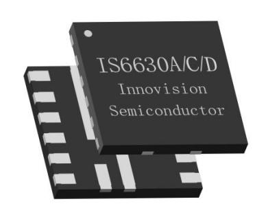
Figure 1 IS6630A / C / D full switch mode converter
●IS6630A With fully integrated VDDQ (BUCK), VTT (LDO), VPP (LDO) and VTTREF power channels; I S6603C / D with fully integrated VDDQ (LDO), VDD 1 (LDO), VDD 2 (BUCK) power channels
● put to use TCOTTMControl mode to achieve a rapid and transient response
●Continuous output current of 10A
● Switch frequency: 500 kHz / 700 kHz
● Excellent load adjustment rate and linear adjustment rate, with an accuracy of 1%
● Under VIN=12V,VOUT=1.2V conditions, the efficiency in the load range can reach more than 92%
● Support internal soft start, programmable valley value flow limit
● Internal integration of OCP, NOCP, OVP, UVLO, OTP and other protection functions
product superiority
1. The control loop is simple, and the transient response speed is extremely fast
IS6630A / C / D using the long industrial micropatent TCOTTMIn control mode, the FB is directly compared with REF to adjust the output voltage, the feedback line makes no complex compensation, there is no RC network delay; and the control loop can respond quickly to the output voltage change without waiting for the clock. Therefore, there is no clock delay, and the transient response speed can be achieved using only a small amount of ceramic capacitor. The following figure shows a schematic comparison of the transient response of the current mode control and the COT control mode. Obviously, the COT control mode is much faster.
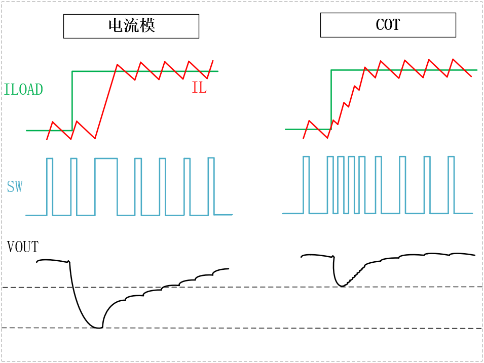
Figure 2 Schematic diagram of the transient response between current mode control and COT control mode
2. RAMP ramp compensation, support for all-ceramic output capacitance
IS6630A / C / D integrates the slope compensation network, namely RAMP signal, inside the chip, which is superimposed on FB to simulate the resistance ripple of ESR and avoid the unstable phenomenon of "multi-pulse oscillation". IS6630A / C / D can work stably with the all-ceramic capacitor, saving space and reducing the cost.
3. Built-in integrator, high output voltage accuracy
IS6630A / C / D introduces a slow digital integrator to continuously correct the reference voltage REF, so as to improve the accuracy of the output voltage and eliminate the half-ripple bias existing in COT. The digital integrator also makes IS6630A / C / D with good linearity, with the output voltage accuracy up to ± 1% at different load current and input voltage.
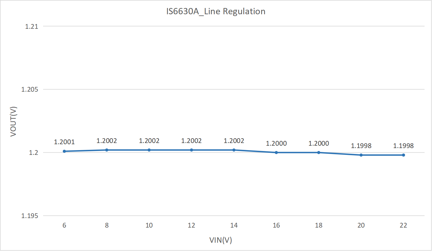
Figure 3 IS6630A
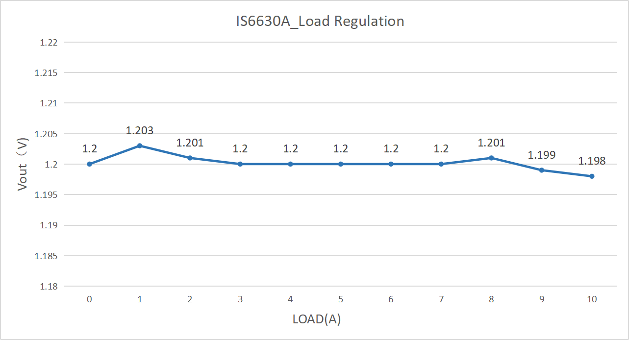
Load adjustment plot of Figure 4 IS6630A
4. High efficiency, low power consumption
Thanks to the technical optimization of integrated MOS tube low on resistance and drive circuit, the efficiency of IS6630A / C / D can be up to 92% under VIN=12V,VOUT=1.2V conditions. Under the condition of light load, the chip is fixed to DCM mode, which further reduces the power consumption of the chip and improves the overall working efficiency of the chip. In addition, the IC also has USM ultrasonic mode: compared with the ordinary DCM mode, open the low side MOS tube more, significantly improve the switching frequency, and avoid the IC light load switching frequency falling into the human ear sound frequency range in the DCM mode, the obvious audible noise.
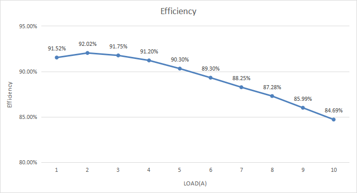
Figure 4 Schematic representation of the efficiency curves for IS6630A / C / D
Series selection
IS6630A / C / D support-40 to + 125℃ ambient temperature, suitable for data transmission rate / wide output voltage range of pen, server, data center and other fields. IS6630 It can provide a variety of three-way output voltage choices, which is conducive to terminal application engineers to design diversified schemes according to different application scenarios.

Figure IS6630A / C / D Specific application classification and required voltmeter
Application scenario instances
The input voltage of the laptop motherboard is determined by the battery specification and the adapter. Generally, the laptop adapter voltage is 19V, and the battery can be divided into 3S (9V-13.2V) and 4S (12V-17.6V). The following takes the 4S battery powered notebook motherboard as an example to introduce the application design example of IS6630A power supply for DDR 4:
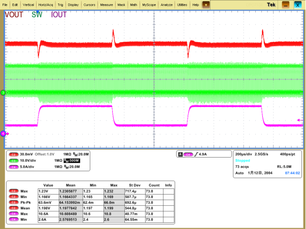
Conditions of application: VIN = 12 V ~ 19V,VOUT=1.2V(Imax=10A),VTT=0.6V(Imax=1A),VPP=2.5V (Imax = 1 A), Load Step: 0A ~7A & 3A ~10A, PKPK of VOUT 120 mV (± 5%).
First select the switch frequency, the IS6630A switch frequency is 500 kHz and 700 kHz respectively, it is generally recommended to choose 700 kHz;
Secondly, the inductance value is determined according to the inductance current ripple is 20%~40% of the full load output current. The full load current is 10A, then the range of the inductance current ripple is 2A ~4A. According to the formula, combined with VOUT=1.2V, Fsw = 700 kHz, calculated VIN = 12 V, the inductance value range is 0.39 uH ~ 0.77 uH, VIN = 19 V, the inductance value range is 0.4 uH ~ 0.8 uH, the final inductance value is 0.68 uH;
Finally, according to the design tool provided by Chang Micro, appropriate output capacitors are selected for VDDQ, VTT and VPP. Here VDDQ uses 622 uF ceramic capacitors, VTT uses 14.7 uF and 122 uF ceramic capacitor in parallel, and 11 uF and 147 uF ceramic capacitor for VPP in parallel. Thus, the key parameters of this application have been determined, and the following is the corresponding measured waveform.
Load Transient: VIN=19V VOUT=1.2V, LOAD 3A~10A 1A/us, PKPK of VOUT=66mV
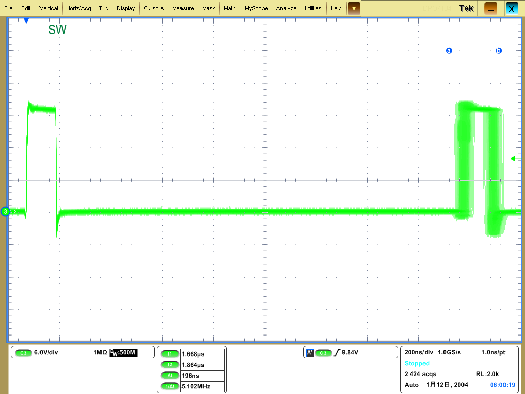
Vo Ripple: VIN=19V VOUT=1.2V, LOAD=10A, PKPK of VOUT=10mV

JITTER of LOAD=5A
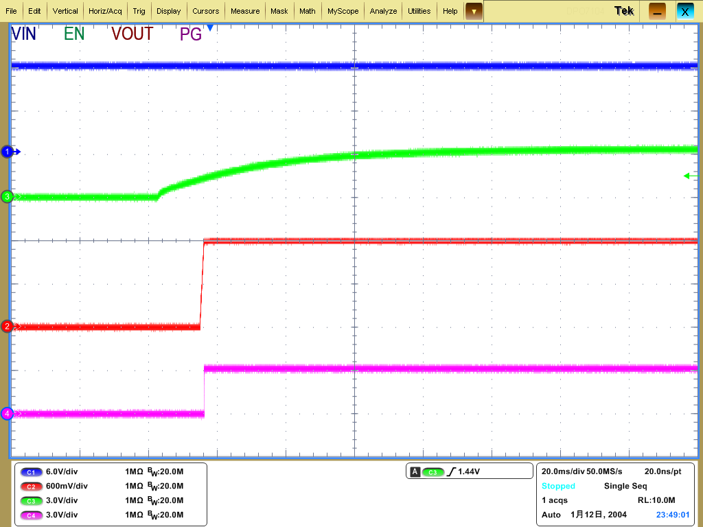
Power on by EN2
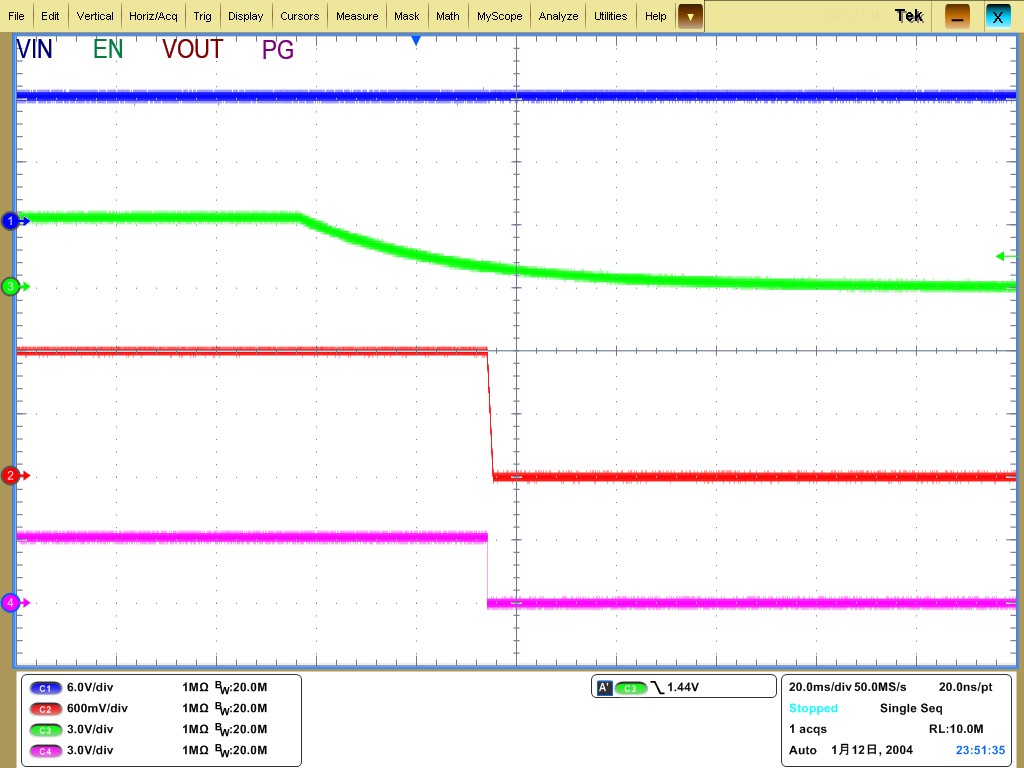
Power off by EN2
[About US]
Innovision Semiconductor Inc. was founded in May 2016, located in Songshan Lake, Dongguan, has a professional technical team, adhere to independent forward research and development, committed to high performance low voltage high current power chip design. In view of the domestic gap in the field of CPU power supply, a full set of solutions, breaking the status quo of foreign chip monopoly. Products include switching power supply, multi-phase controller, intelligent power level, power module, etc., which can be widely used in server, computer, communications, consumer electronics and other markets.

